A Raspberry Pi 5 wants a steady 5 volts at up to 5 amperes, more than most phone chargers can give it. This project builds that supply from scratch on perforated board: a transformer, a rectifier, filter capacitors, a switching regulator, an over-voltage "crowbar" and a USB-C lead that tells the Pi how much current it may draw. Every part is explained from the start, so you can follow along even if you have never built a power supply before, and every number is worked out so you can check it.
Read this first: this project connects to household mains (120 V AC). Mains voltage can kill. The low-voltage half of the circuit is a good learning build; the mains half (the inlet, fuse F1 and the transformer's primary) needs care, insulated joints, a fused inlet with an earth wire and a careful first power-up through a dim-bulb tester (section 15). If you are not confident working with mains wiring, build the low-voltage half and feed it from a ready-made, certified 12 V AC or 15 to 20 V DC adapter instead. See section 17, Safety.
How to use this page. Sections 1 to 10 explain what each part of the supply does and why. Section 11 has the full schematic, section 12 the parts list, and sections 13 to 16 the build, testing and set-up. Numbers on this page that carry no source number were worked out with the formulas shown.
1. Why the Pi 5 needs 5 V at 5 A
Three words come up all the time in this project. Voltage (measured in volts, V) is the electrical "push" that drives current around a circuit. Current (amperes, or amps, A) is how much electric charge flows past a point each second. Power (watts, W) is how fast energy is delivered: volts times amps. If those are new to you, the Ohm's Law and Power (PIE) Formula helpers explain them with calculators.
The Raspberry Pi 5 is a small computer that runs from 5 V. The Raspberry Pi documentation recommends a supply that can deliver 5 A for the Pi 5, and the official supply is a 27 W USB-C unit.[1] Five volts at five amps is 5 × 5 = 25 W. Not all of that goes to the Pi's own chips: the Pi passes power on to whatever you plug into its USB ports (drives, cameras, keyboards). With a supply it trusts for 5 A, the Pi lets its USB ports draw up to 1.6 A in total; with any other supply, it limits them to 600 mA (0.6 A).[1]
Under-voltage is what happens when the supply can't keep up. Every wire and connector has a little resistance, and by Ohm's law a current through a resistance loses some voltage (E = I × R). At 5 A, a cable with just 0.05 Ω in it loses 0.25 V. The Pi watches its input and flags a warning if it falls below 4.63 V (±5 %, so somewhere between about 4.40 and 4.86 V).[1] When that happens it slows its processor down ("throttles") to cut its own power draw, and the documentation warns that a poor supply can corrupt storage or cause unpredictable behavior.[1] This supply aims a little high, 5.13 V at its output terminals, so that after the cable losses the Pi still sees about 4.9 to 5.0 V at full load.
2. The plan: one stage at a time
The wall socket gives alternating current (AC): a voltage that swings from positive to negative and back, 60 times a second in North America. Its "120 V" is an average-like value called RMS; the peaks reach about 170 V. The Pi needs direct current (DC): a steady voltage that does not change direction. Getting from one to the other takes several stages, shown in Figure 1. Each box is one section of this page.
In words: the transformer steps 120 V AC down to about 12 V AC and isolates the rest of the circuit from the mains. The rectifier flips the negative half of each AC cycle so that all of it points the same way. The filter capacitors smooth those bumps into fairly steady DC of about 15 to 21 V. The buck regulator converts that to a precise 5.13 V without wasting much energy as heat. The crowbar protects the Pi if anything goes wrong, the fuses protect the wiring, and the USB-C lead delivers the power and tells the Pi how much it can safely take.
Why not just buy the official 27 W supply? You can, and for most people you should. This build exists because it is a good way to learn how a real power supply works, because a linear-transformer front end is quiet and very robust, and because you end up with a supply you understand completely and can repair.
3. Stage 1: the mains inlet, fuse F1 and the earth wire
Mains power comes in through J1, a standard IEC inlet: the same three-pin socket found on the back of a computer, which takes an ordinary detachable power cord. The one used here (Qualtek 719W-00/02) has a built-in drawer for a 5 × 20 mm fuse. A fuse is a thin wire designed to melt and break the circuit if too much current flows; fuse F1 here is rated 1 A. It is a slow-blow (time-delay, marked "T") type, which ignores the short surge of current at switch-on but still opens on a lasting fault. See Fuses and Circuit Protection for more.
The three pins are line (also called live or hot: the one carrying the 120 V), neutral (the return, near earth potential) and protective earth (PE, the green/yellow wire, connected to the ground rod at your electrical panel). The fuse must be in the line wire, so that when it blows the circuit after it is disconnected from the live side.
The earth wire is there for faults. Because this supply lives in a plastic (3D-printed) case, there is no metal box to earth. Instead, PE is connected to the 0 V (negative) side of the low-voltage circuit at one point. The transformer is already built to keep mains and low voltage apart (it is tested at 4000 V between them[7]), so this is a second layer of protection: if a loose mains wire ever touched the low-voltage side, the fault current would flow to earth and blow F1, instead of making the Pi's metal parts live.
4. Stage 2: the transformer
A transformer is two (or more) coils of wire wound on a shared iron core. AC in the first coil, the primary, makes a changing magnetic field in the core, and that field produces an AC voltage in the second coil, the secondary. The voltage ratio follows the ratio of turns: fewer turns on the secondary means a lower voltage. The two coils are not connected by any wire, so the secondary is isolated from the mains. Transformers covers how this works.[13]
T1 is a Triad Magnetics VPP24-2330, rated 56 VA (volt-amperes, close to watts for this purpose). It has two 115 V primaries and two 12 V secondaries, so it can work on 115 V or 230 V mains. For 120 V, the datasheet connects the two primaries in parallel (side by side: pins 1 and 4 joined, and pins 3 and 6 joined), and the two 12 V secondaries also in parallel (7 with 10, 9 with 12) for 12 V at up to 4.66 A.[7]
Phasing matters. Each winding has a "start" end, marked with a dot on the schematic (pins 1, 4, 7 and 10). Parallel windings must be joined start to start and end to end. Get one backwards and the two windings fight each other: it is a dead short across the mains (primaries) or across 24 V (secondaries), the fuse blows, and the transformer can be damaged. The build notes give a safe meter check before you close each pair of jumpers.
The "12 V" rating is at full load. A transformer's output sags as you draw more from it, because of the resistance of its copper windings; Triad rates this one at 25 % regulation, meaning the no-load voltage is about 25 % higher than the full-load voltage.[7] With nothing connected you will measure about 15 to 16 V AC on the secondary, which is normal.
5. Stage 3: the bridge rectifier
A diode is a one-way valve for current: it conducts in one direction (from its anode to its cathode) and blocks the other. Four diodes arranged in a diamond, called a bridge rectifier, steer both halves of the AC cycle into the same direction at the output. The result is DC that still bumps up and down 120 times a second. Diodes explains rectifiers with diagrams.[14]
BR1 is a GBPC3510W, a four-diode bridge in one block, rated 35 A and 1000 V.[11] That is far more than needed; it was chosen because its big metal base bolts to a heatsink and its wire leads suit perf board. The current always passes through two diodes, each dropping about 0.8 to 1 V, so at about 3 A average the bridge turns roughly 4 W into heat (up to about 6 W at low mains voltage). In this plastic case it gets its own finned aluminum heatsink. Its metal base is electrically isolated from the diodes, so the heatsink is not live.[11]
6. Stage 4: filter capacitors
A capacitor stores electric charge, a bit like a small, fast rechargeable tank. Placed across the rectifier output, big capacitors fill up at each peak and supply the current in between, smoothing the bumps into fairly steady DC. The leftover wobble is called ripple. See Capacitors.
C1, C2 and C3 are 2200 µF (microfarads) each, rated 35 V, for 6600 µF in total. With nothing connected the capacitors charge to the peak of the AC, about 21 V (up to about 23 V if your mains runs high at 132 V). At full load the average falls to about 14.6 V with a volt or two of ripple. The regulator after them only needs about 8 V to work, so there is plenty of margin. Electrolytic capacitors like these have a polarity: the stripe marks the negative lead, and they must go in the right way round.
R8, a 10 kΩ resistor, is a bleeder: it slowly drains the capacitors after you unplug, so the board isn't left charged. Its time constant is 10 kΩ × 6600 µF ≈ 66 seconds, so give it about five minutes before working on the board.
7. Stage 5: the buck regulator
A voltage regulator holds its output at a fixed voltage even when the input voltage or the load changes. The simplest kind, a linear regulator, works like a variable resistor that burns off the extra voltage as heat. Dropping 15 V to 5 V at 5 A that way would waste 10 V × 5 A = 50 W, twice the power delivered to the Pi. Instead, this supply uses a switching or buck regulator. See Voltage Regulators.
A buck regulator switches its input on and off very fast (here 260,000 times a second, 260 kHz) and smooths the pulses with an inductor and capacitors.[5] An inductor is a coil that resists changes in current, so it keeps current flowing smoothly between pulses. The fraction of time the switch is on (the duty cycle) sets the output: on about a third of the time, 15 V in averages to 5 V out. Because the switch is either fully on or fully off, it wastes little power, and this supply's buck stage is roughly 85 to 90 % efficient.
The parts of the buck stage:
- U1, LM2678T-ADJ (Texas Instruments): the controller and power switch in one 7-pin package, rated 5 A. Its pins are 1 switch output, 2 input, 3 boost capacitor, 4 ground (also the metal tab), 5 not connected, 6 feedback and 7 on/off.[5] Pin 7 is left unconnected, which keeps the regulator on.
- L1, 22 µH, 6.7 A: the inductor.
- D1, MBR1045G: a Schottky diode (a fast diode with a low voltage drop) that carries the inductor current while U1's switch is off. It is often called the catch diode. Its metal tab is the cathode.[9]
- C4 and C5, 560 µF each: output capacitors. TI's design table calls for two 560 µF, 35 V low-impedance capacitors for a 5 V output with a 22 µH inductor.[5]
- C3 (2200 µF) and C7 (0.1 µF) right at U1's input pins, and C6 (0.01 µF) from pin 3 to pin 1, which U1 uses to drive its internal switch.[5]
Setting the voltage. U1 adjusts its switching until its feedback pin sits at 1.21 V. Two resistors form a voltage divider from the output: R2 (3.24 kΩ) on top and R1 (1.00 kΩ) on the bottom. The datasheet formula is[5]
Vout = 1.21 V × (1 + R2 ÷ R1) = 1.21 × (1 + 3.24 ÷ 1.00) = 1.21 × 4.24 ≈ 5.13 V
The reference can be anywhere from 1.186 to 1.234 V,[5] so a given chip will land between about 5.03 and 5.23 V. If the Pi reports under-voltage at heavy load, adding a resistor across R1 raises the output: 56 kΩ gives about 5.20 V and 33 kΩ about 5.25 V.
The "hot loop". The current through C3, U1 and D1 switches on and off in a few billionths of a second. Long wires in that loop act like antennas and add voltage spikes, so these three parts sit right next to each other with short, heavy wires. This is the single most important layout rule for the build.
Heat: U1's metal tab is its ground pin, so its heatsink (HS1) is at 0 V and needs no insulation. D1's tab, though, is its cathode, which is the switching node: its heatsink (HS2) carries a 0 to 23 V square wave and must not touch anything else.
8. Stage 6: the crowbar (over-voltage protection)
If the regulator ever failed with its switch stuck on, the full 15 to 23 V would reach the Pi and destroy it. A crowbar circuit guards against that. It watches the output, and if the voltage goes too high it deliberately short-circuits the supply, like dropping a metal bar across the terminals. The short blows fuse F2, and the Pi is saved.
Three parts do the work:
- U2, TL431: an adjustable shunt reference. It does nothing until the voltage on its REF pin reaches 2.495 V, then it suddenly conducts.[6] A divider (R3 + R4 = 13.24 kΩ on top, R7 = 10.0 kΩ below) sets the output voltage at which that happens:
Vtrip = 2.495 V × (1 + 13.24 ÷ 10.0) ≈ 5.80 V
With the TL431A's tolerance and 1 % resistors, that is about 5.7 to 5.9 V: well above the normal 5.13 V, and below the Pi's limit. - Q2, 2N3906: a small PNP transistor, a current-controlled switch. When the TL431 conducts it pulls current out of Q2's base (through R10, 1 kΩ), which switches Q2 on.[10]
- Q1, 2N6504: a silicon controlled rectifier (SCR or thyristor), a heavy switch that, once its gate gets a small push of current, turns on and stays on until the current through it stops.[15] Q2 feeds it about 46 mA through R9 (100 Ω); the datasheet says at most 30 mA is needed at room temperature.[8] Q1 sits across the regulator's input, after F2. It can carry a 250 A surge,[8] so it simply holds the short while F2 melts.
R5 (1 kΩ) and C8 (0.1 µF) from Q1's gate to its cathode keep electrical noise from firing it by accident.
A design lesson. The first version of this circuit drove the SCR's gate straight from the TL431. It looks fine, but the TL431 measures its 2.495 V from REF to its own anode pin,[6] and with the anode on the SCR gate that pin sits about 1 V above ground. The real trip point would have been around 7.4 to 9.3 V, too high to save the Pi. Grounding the TL431's anode and adding Q2 fixed it. Always check what a part's reference voltage is measured against.
9. The fuses
Two fuses protect different things. F1 (1 A slow-blow, in the inlet drawer) protects the mains wiring and the transformer. At full load the primary draws about 0.4 to 0.5 A, so 1 A leaves room for the switch-on surge; a short on the secondary side pulls about 3 A from the mains and blows it within seconds. F2 (4 A slow-blow, in a board-mounted holder) protects the low-voltage side and is the fuse the crowbar blows. In normal use the current through it is about 2 to 3.3 A, depending on load and mains voltage.
Use the power formula (PIE) to check: 26 W out of the regulator at about 88 % efficiency is about 30 W in; at 14.6 V that is 30 ÷ 14.6 ≈ 2.1 A. Fuses are normally run at no more than about 75 % of their rating for long life, so if you will run the Pi at a sustained 5 A on low mains, a 5 A fuse is a reasonable swap. Always replace a blown fuse with the same type and rating, and find out why it blew first. Fuses and Circuit Protection covers fuse ratings in depth.
10. The USB-C lead and the CC wire
The output reaches the Pi through a captive USB-C lead: a good-quality 5 A USB-C cable (Tripp Lite U040-003-C-5A) cut in half, with the cut end wired to the board. Inside a USB-C cable are the power pair (VBUS, positive, and GND), the data wires (D+ and D−, plus high-speed pairs) and a configuration channel wire, CC.
A USB-C power source tells the device how much current it offers using a resistor from CC to VBUS. The USB Type-C specification defines a 10 kΩ pull-up (to a 5 V supply) as "3.0 A available".[12] The Pi has its own 5.1 kΩ resistor from CC to ground, and the voltage it sees across that one (about 1.7 V) tells it which level is on offer. So: VBUS and GND carry the power, CC gets R6 (10 kΩ) to VBUS, and every data wire is cut short, insulated and left unconnected. Find the CC wire with a meter: it is the one with continuity to pin A5 on the plug.
Why 3 A, when the supply can give 5 A? The only way to advertise 5 A at 5 V is USB Power Delivery (PD), a digital conversation over the CC wire that needs a dedicated chip. The Pi accepts the 3 A signal and runs normally, but limits its USB ports to 600 mA unless you tell it otherwise in its configuration file (section 16).[1][2]
11. The schematic
A schematic is a circuit's wiring diagram, using symbols instead of pictures of the parts. Each part has a reference designator (R1, C3, U1 and so on) that matches the parts list. Lines are wires, and a dot where lines meet means they are connected; lines that cross without a dot are not. Every ground symbol is the same 0 V connection. The red dashed box is the mains section. The schematic is wide; scroll sideways on a small screen, or open the full-size version.
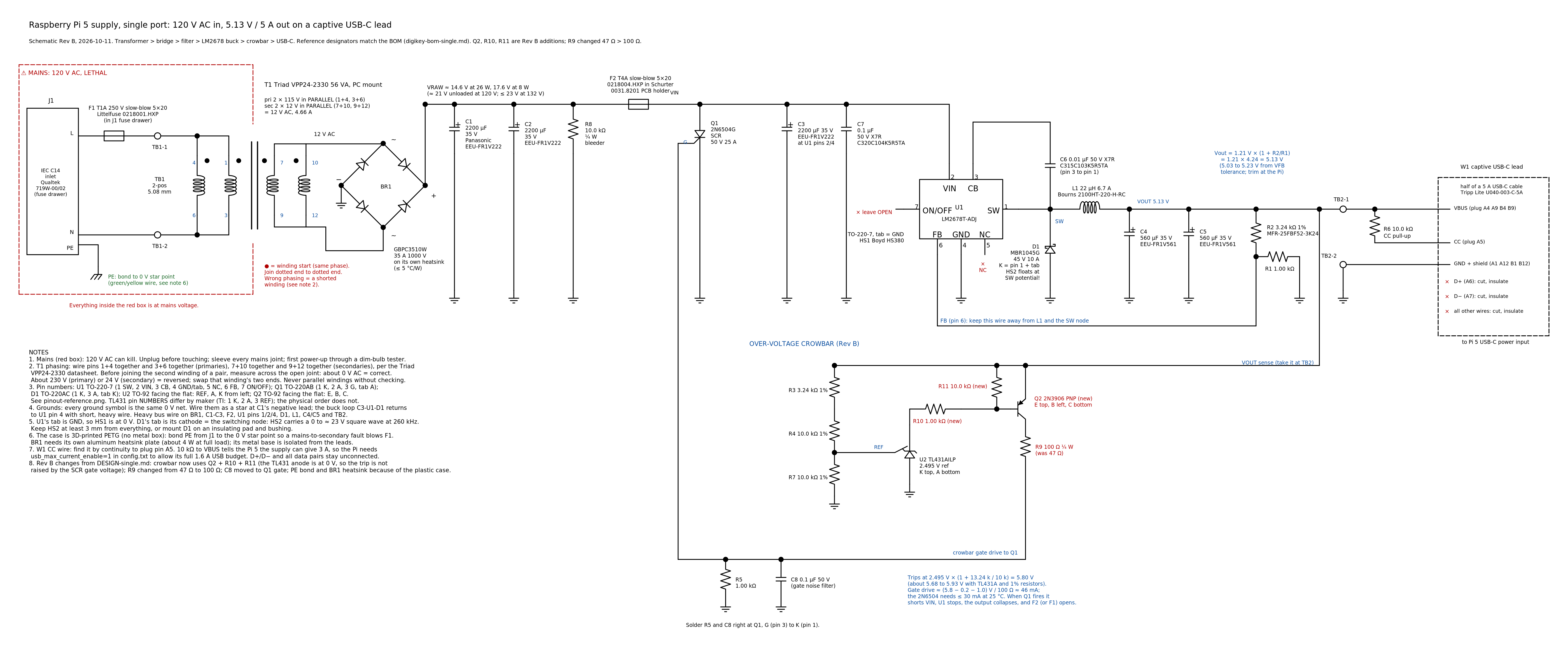
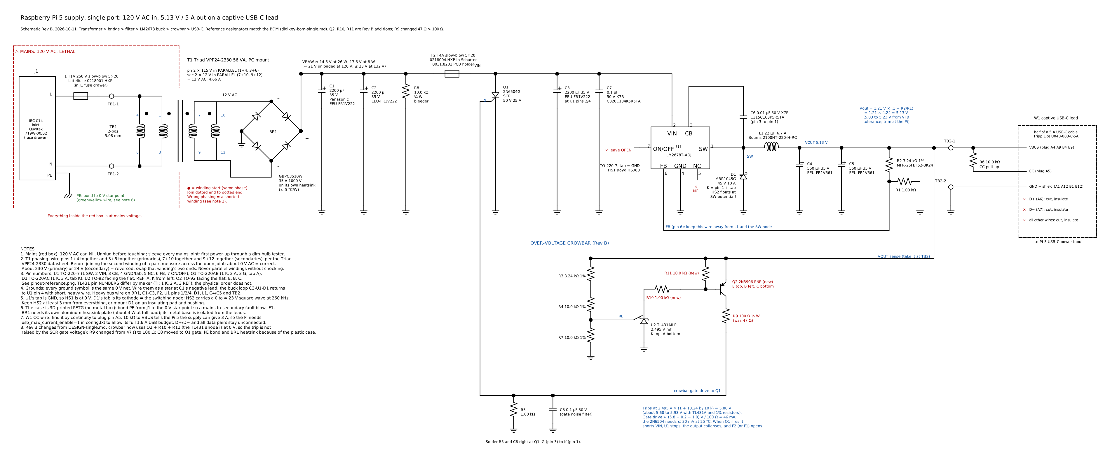
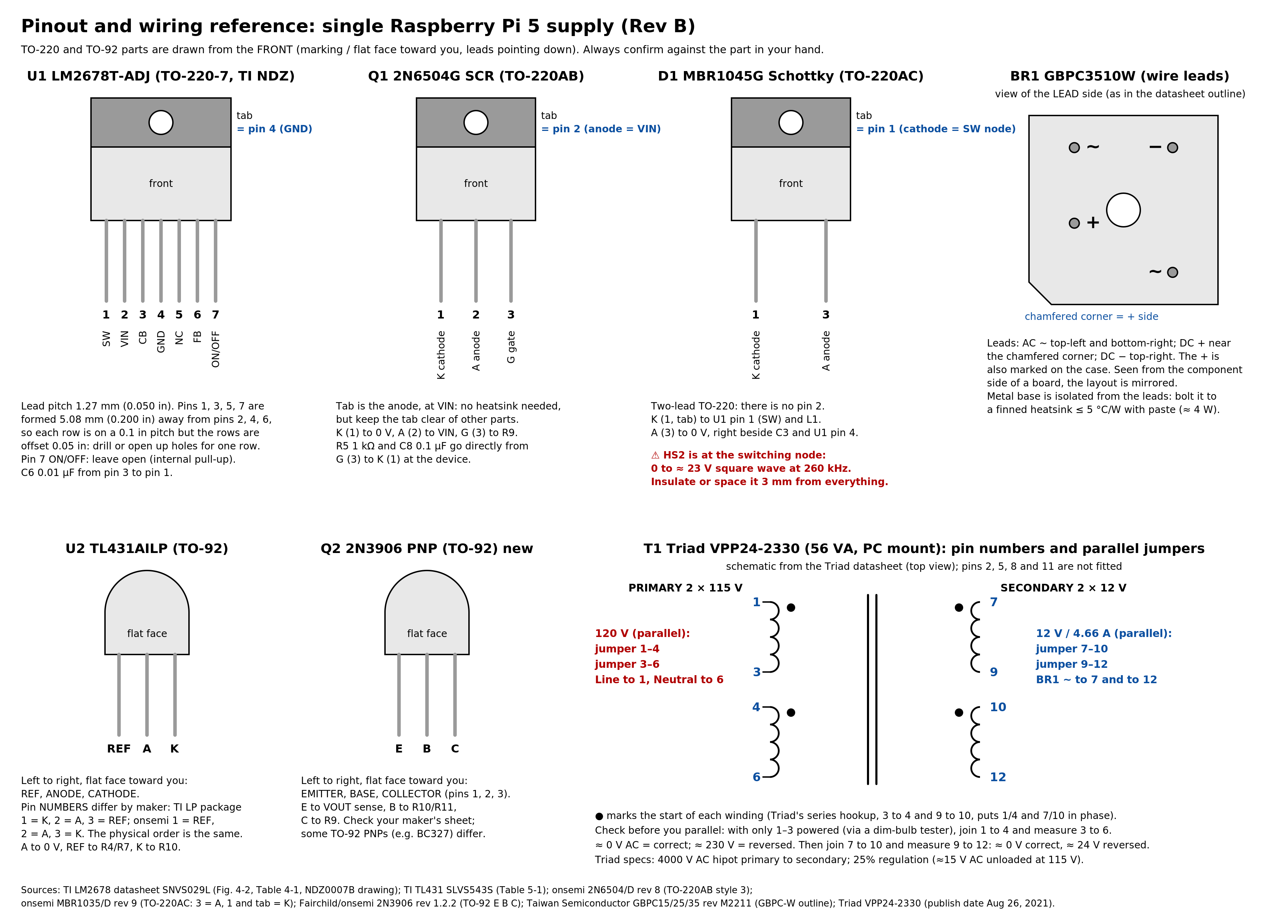
Figure 3 shows where each pin is on the actual parts, which is where most build mistakes happen. TO-220 and TO-92 parts are drawn looking at the front (the printed side) with the leads pointing down. Note the TL431: different makers number its pins differently, but the physical order is the same.[6]
12. Parts list
Part numbers are as ordered from DigiKey. Resistors are 1 %, ¼ W metal film unless noted. The perf board, terminal blocks and cable are interchangeable with anything of similar rating.
| Ref | Qty | Part | Value / rating | Role |
|---|---|---|---|---|
| J1 | 1 | Qualtek 719W-00/02 | IEC C14 inlet with fuse drawer, 10 A | Mains in |
| F1 | 1 | Littelfuse 0218001.HXP | T1A 250 V, 5 × 20 mm | Mains fuse |
| T1 | 1 | Triad VPP24-2330 | 56 VA, 2 × 115 V / 2 × 12 V | Transformer |
| BR1 | 1 | Taiwan Semi GBPC3510W | 35 A 1000 V bridge | Rectifier |
| HS3 | 1 | Aluminum heatsink | ≤ 5 °C/W | For BR1 |
| C1–C3 | 3 | Panasonic EEU-FR1V222 | 2200 µF 35 V | Filter / U1 input |
| R8 | 1 | YAGEO MFR-25FBF52-10K | 10.0 kΩ | Bleeder |
| F2 | 1 | Littelfuse 0218004.HXP + Schurter 0031.8201 holder | T4A 250 V | DC rail fuse |
| U1 | 1 | TI LM2678T-ADJ/NOPB | 5 A buck, TO-220-7 | Regulator |
| L1 | 1 | Bourns 2100HT-220-H-RC | 22 µH 6.7 A | Buck inductor |
| D1 | 1 | onsemi MBR1045G | 45 V 10 A Schottky | Catch diode |
| C4, C5 | 2 | Panasonic EEU-FR1V561 | 560 µF 35 V | Output filter |
| C6 | 1 | KEMET C315C103K5R5TA | 0.01 µF 50 V X7R | U1 boost |
| C7, C8 | 2 | KEMET C320C104K5R5TA | 0.1 µF 50 V X7R | U1 input bypass; Q1 gate filter |
| R1 | 1 | YAGEO MFR-25FBF52-1K | 1.00 kΩ | Feedback divider (bottom) |
| R2 | 1 | YAGEO MFR-25FBF52-3K24 | 3.24 kΩ | Feedback divider (top) |
| U2 | 1 | TI TL431AILP | 2.495 V shunt reference, TO-92 | Crowbar sensor |
| R3, R4, R7 | 3 | 3.24 kΩ, 10.0 kΩ, 10.0 kΩ | 1 % | Crowbar divider |
| Q2 | 1 | onsemi 2N3906BU | PNP 40 V 200 mA, TO-92 | Crowbar driver |
| R10, R11 | 2 | 1.00 kΩ, 10.0 kΩ | 1 % | Q2 base, base pull-up |
| R9 | 1 | YAGEO MFR-25FBF52-100R | 100 Ω | SCR gate current |
| R5 | 1 | YAGEO MFR-25FBF52-1K | 1.00 kΩ | SCR gate–cathode |
| Q1 | 1 | onsemi 2N6504G | SCR 50 V 25 A, TO-220 | Crowbar switch |
| R6 | 1 | YAGEO MFR-25FBF52-10K | 10.0 kΩ | USB-C CC pull-up |
| HS1, HS2 | 2 | Boyd 530002B02500G | TO-220 heatsink | U1, D1 |
| TB1, TB2 | 2 | Phoenix Contact 1729128 | 2-pos 5.08 mm | Mains in; DC out |
| W1 | 1 | Tripp Lite U040-003-C-5A | USB-C 5 A cable, cut | Captive lead |
| — | 1 | Perf board, bus wire, thermal paste, M3 hardware | — | Construction |
13. Construction
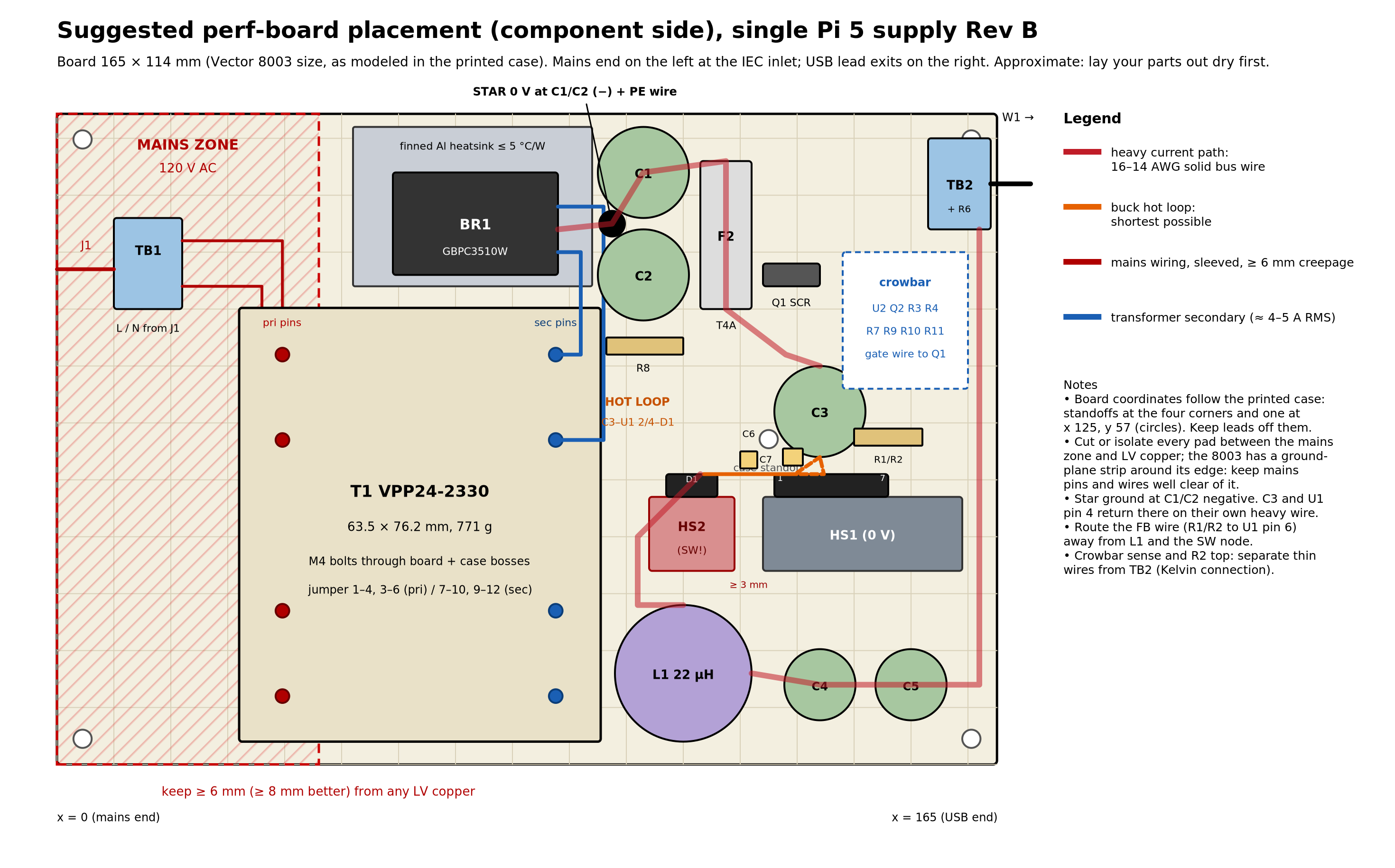
The board is 165 × 114 mm (6.5 × 4.5 in) perf board: board with a grid of holes, each with its own copper pad, so you make every connection yourself with wire and solder. Figure 4 shows the suggested layout. The mains parts sit at the left end, well away from everything else, and the output terminal is at the right end next to where the USB-C lead leaves the case.
Key rules:
- Keep mains apart. Leave at least 8 mm of bare board between any mains connection and anything on the low-voltage side; cut away copper pads along that line. Cover every mains joint with heat-shrink tubing, and tie wires down so a broken joint cannot swing loose.
- Heavy wire for heavy current. The path from the transformer through the rectifier, capacitors, regulator, inductor and out to the terminal carries 3 to 5 A. Use 16 to 18 AWG wire or doubled bus wire, not thin hookup wire.
- Tight hot loop. C3, U1 and D1 as close together as possible, leads short (section 7).
- Star ground. Run all the 0 V (ground) wires back to one point, at the negative leads of C1 and C2. This keeps the big switching currents from disturbing the small feedback and crowbar signals.
- Sense at the terminal. Connect the top of the feedback divider and the crowbar's sense wire at the output terminal TB2, so the 5.13 V is set where it leaves the board.
- Insulate D1's heatsink. Mount D1 on an insulating pad and shoulder washer, or keep its heatsink at least 3 mm from everything.
- LM2678 leads. Its seven leads are only 1.27 mm apart and formed into two staggered rows. On 2.54 mm (0.1 in) perf board, drill the odd-numbered row between grid holes or gently spread the leads.
- Secure the transformer. It weighs about 0.8 kg (1.7 lb)[7]; use its mounting holes and a couple of cable ties, not just its solder pins.
The full builder's notes, with exact coordinates and a wiring order, are published with this project's downloads.
14. The 3D-printed case
The supply lives in a two-piece case printed in PETG, a tough plastic that copes with the warmth inside (about 50 °C at full load; PETG softens at around 80 °C). The case has mounting bosses for the transformer, standoffs for the board, a cut-out for the IEC inlet, an exit for the USB-C lead, ventilation slots and an internal barrier between the mains end and the rest of the board. It replaces the Hammond 1590EE metal box in the original design. Because it is plastic, the earth wire is bonded as described in section 3.
Case status: in progress. The case is designed and the printable files are below. The pictures in this section are computer renders of the design, not photos; photos of the printed case with the board installed will be added as the build goes along.
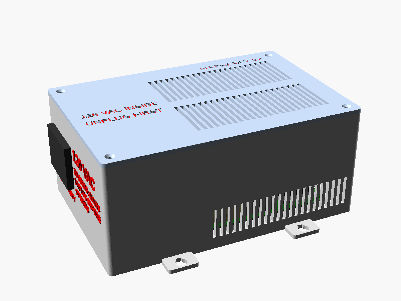
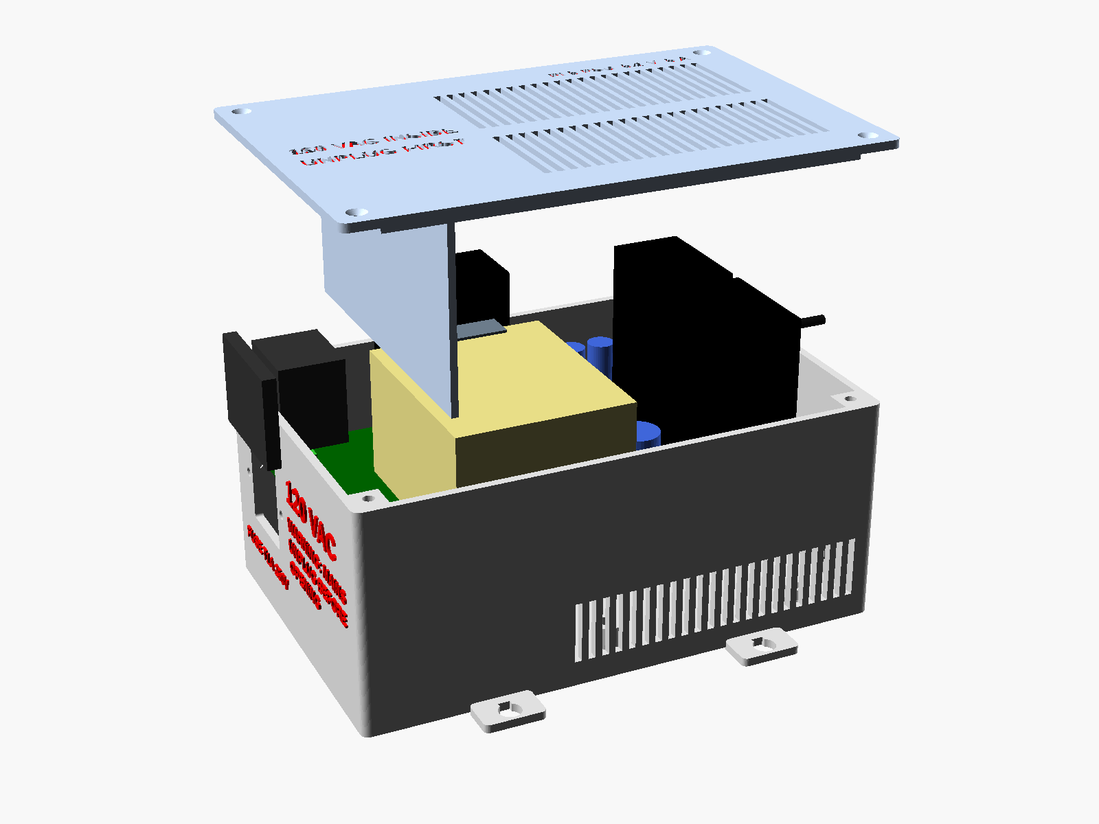
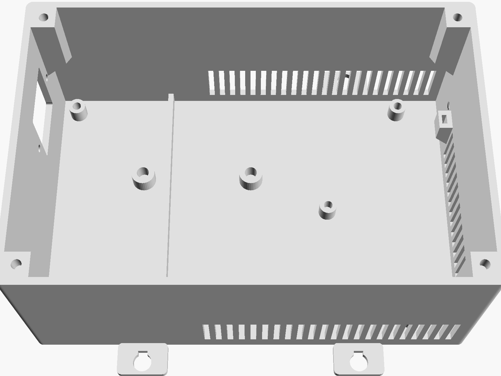
What the case provides
- Size. The base tub is 190 × 126 × 81 mm on the outside (about 7.5 × 5.0 × 3.2 in), 84 mm tall with the lid on, and 154 mm wide across the wall tabs. Walls, floor and lid are 3 mm thick.
- Board mounting. The 165 × 114 mm perf board sits on five 8 mm standoffs, one at each corner and one under the buck regulator area, with M3 heat-set inserts (threaded inserts you press into the plastic with a soldering iron). The board coordinates match the placement sketch in Figure 4.
- Transformer mounting. Four larger bosses with M4 heat-set inserts match the transformer's mounting-hole pattern (2.0 × 2.5 in), so the 0.8 kg transformer bolts through the board into the case[7].
- Lid. Four countersunk M3 screws go into inserts in corner blocks. A 3 mm lip locates the lid.
- IEC inlet. A rectangular cut-out in the mains end wall, sized from the Qualtek drawing, with two 3.5 mm holes for countersunk M3 screws and nuts.
- USB-C exit. A 4.3 mm hole for the 3.8 mm cable at the other end. Inside, a cable tie through a small anchor block acts as the strain relief: the tie's head stops the cable pulling out.
- Ventilation. Side and end slots low down let cool air in (about 33 cm²) and lid slots over the regulator half let warm air out (about 46 cm²). There are no vents at the mains end. At full load the inside air is calculated to run about 17 °C above room temperature.
- Mains barrier. A rib hanging from the lid and a low rib under the board separate the inlet, fuse and transformer primary area from the low-voltage side.
- Labels. Raised text at the mains end ("120 VAC", "WARNING: MAINS / UNPLUG BEFORE / OPENING", "FUSE T1A 250V") and the USB end ("5.1 V USB-C / 5 A MAX"); recessed text on the lid ("120 VAC INSIDE / UNPLUG FIRST" and "PI 5 PSU 5.1 V 5 A").
- Feet and mounting. Shallow pockets for four 12.7 mm (½ in) stick-on rubber bumpers, and four keyhole tabs for screwing the case to a wall or shelf.
The bridge rectifier can't use a metal case wall as its heatsink, so in this design it bolts to its own finned aluminum heatsink beside the transformer (section 5).
Printing it
The case was set up for an Anycubic Kobra 2 Pro (220 × 220 mm bed). The base and lid don't fit on the bed together, so each is printed separately, with no supports: the base open side up, the lid top face down.
| Part | Print time (estimate) | Filament (estimate) |
|---|---|---|
| Base tub | 15 h 32 min | 254 g |
| Lid | 5 h 13 min | 88 g |
| Total | about 20 h 45 min | about 342 g |
- Material: PETG, 1.75 mm (the slicer profile uses Geeetech metallic blue PETG). PLA is not recommended: the inside air can reach about 47 °C (in a 30 °C room) and the transformer's surface about 75 to 80 °C at sustained full load, above PLA's softening point of about 60 °C.
- Settings used: nozzle 245 °C for the first layer then 240 °C; bed 80 °C then 78 °C; 0.2 mm layers; 4 perimeters; 5 top and 4 bottom layers; 25 % gyroid infill; part-cooling fan about 30 %.
- Bed release: PETG bonds very hard to a PEI sheet. Wipe it with isopropyl alcohol, add a thin layer of glue stick as a release, and let the plate cool before flexing it.
- Dry the filament if the spool has been open for more than a week: 80 °C for 4 to 6 hours, or 65 °C if the spool itself starts to distort.
The plastic is not the insulation. Ordinary PETG is not flame-rated to the standard of a commercial power-supply case (it is typically UL94 HB, not V-0), and metallic PETG contains metal-effect pigment. Every live part must be insulated in its own right: sleeve every inlet tab and splice, and keep the mains wiring on the mains side of the barrier ribs. A flame-retardant PETG or PC-ABS rated UL94 V-0 at 3 mm is a better choice if you can get it. Never run the supply with the lid off. See section 17.
Hardware for the case
Not in the DigiKey parts list (builder's stock):
- 9 × M3 × 5.7 mm heat-set inserts (5 for the board, 4 for the lid) and 4 × M4 × 8.1 mm inserts (transformer).
- 5 × M3 × 6 mm pan-head screws (board), 4 × M3 × 10 mm countersunk screws (lid), 4 × M4 × 16 mm screws and washers (transformer; one carries the earth ring lug and a star washer).
- 2 × M3 × 10 mm countersunk screws and nuts (inlet), 1 × M5 × 12 mm screw and nut (bridge rectifier to its heatsink).
- A 2.5 mm cable tie, four 12.7 mm adhesive bumpers and heat-shrink tubing.
Check before you drill. The transformer's mounting-hole pattern comes straight from its datasheet, but the positions of its pins inside each pin row were inferred from the drawing. Hold the real transformer against the board as a drilling template. Also keep the board clear of anything taller than 1.5 mm along the line under the lid's barrier rib, about 30 mm from the mains end of the board.
Downloads
| File | What it is | Size |
|---|---|---|
| pi5psu-case-base.stl | Base tub, STL, already in print orientation | 3.4 MB |
| pi5psu-case-lid.stl | Lid, STL, already in print orientation (top face down) | 1.6 MB |
| pi5psu_case.scad | OpenSCAD source. Every dimension is a parameter, so you can change the board size, hole positions or standoff height to suit your own board. | 15 KB |
15. Testing, step by step
Never connect the Pi until every step below has passed. Test in stages, so that a mistake costs a fuse rather than a Raspberry Pi. You need a multimeter, a dim-bulb tester (an ordinary 40 to 60 W incandescent bulb wired in series with the mains feed, so that a short just lights the bulb instead of blowing fuses or parts), and ideally a bench power supply with a current limit.
- Before power. With the board unplugged, measure resistance: mains line and neutral to earth should read open (more than 10 MΩ). The DC rail should not read as a short to ground.
- First power, through the dim bulb, with U1 and Q1 not yet fitted. The bulb should flash briefly and then go dark or glow dimly. A steady bright bulb means a short or a reversed transformer winding: unplug and check.
- Transformer output. About 15 to 16 V AC across the secondary with no load (higher than 12 V is normal, section 4).
- Raw DC. About 20 to 21 V DC across C1 at 120 V mains. Unplug and watch it drain slowly through R8.
- Fit U1 and set the output. Unplugged and discharged, fit U1. At no load, the output terminal should read 5.03 to 5.23 V (typically 5.13 V).
- Load test. Remove the dim bulb. Connect a 1 Ω, 50 W power resistor on a heatsink (or an electronic load set to 5 A) for a few minutes at a time. The output should stay above about 5.05 V, and nothing should get too hot to keep a finger on for a few seconds.
- Crowbar test, with a bench supply. Unplug mains and remove U1. Fit Q1. Connect a bench supply to the output terminal, current limit 100 mA, starting at 5 V. Raise it slowly: at about 5.8 V the current jumps from almost nothing to about 50 mA. That shows the crowbar trips at the right voltage. To see the SCR latch, also feed the DC rail from a second supply at 12 V limited to 200 to 500 mA: when the output supply passes 5.8 V, the rail collapses to about 1 V and stays there. Keep this test short, then refit U1.
- At the Pi. Only now plug in the Pi. Measure the voltage at the Pi itself (between a 5 V pin and a ground pin on its GPIO header) while it is busy, and check the Pi's own report (section 16).
16. Telling the Pi: config.txt
Because the USB-C lead advertises 3 A (section 10), the Pi limits its USB ports to 600 mA. This supply really can deliver 5 A, so you can lift that limit by adding one line to the Pi's config.txt, a settings file the Pi reads when it starts:[2]
usb_max_current_enable=1On Raspberry Pi OS the file is /boot/firmware/config.txt. On Home Assistant OS it is on the small boot partition (named hassos-boot) of the SD card or SSD; shut down, put the card in another computer and edit it there. Only add this line with a supply that really can provide 5 A, like this one.
Checking for under-voltage. On Raspberry Pi OS, run
vcgencmd get_throttled
vcgencmd pmic_read_adc EXT5V_V
The first command should print throttled=0x0. A 1 in the lowest bit (0x1) means under-voltage right now; 0x10000 means it has happened since the last boot.[3] The second reads the Pi's own measurement of its input voltage, which should stay above about 4.9 V.[1] For a proper test, load the processor with stress-ng --cpu 4 --timeout 600s while your USB devices are busy, and watch both readings.
In Home Assistant, add the Raspberry Pi Power Supply Checker integration (Settings → Devices & services → Add integration). It creates a binary sensor that shows a problem if the Pi running Home Assistant detects under-voltage.[4] Leave it on your dashboard for a few days after building the supply.
17. Safety
- Mains can kill. Unplug before touching the board, every time. Never work on the mains section live. Use one hand and insulated probes when measuring a powered board.
- Earth and fuse. Always use the fused, earthed IEC inlet with the correct T1A fuse. Never bypass a fuse or fit a bigger one to "fix" it blowing.
- Capacitors hold charge. Wait about five minutes after unplugging (or measure) before touching the DC side.
- Heat. BR1, U1, D1 and T1 get warm. Keep the case's vents clear and don't run it in a closed cabinet or in direct sun.
- Phasing. Check transformer phasing before closing the parallel jumpers (section 4).
- Test before the Pi. Do every step of section 15, including the crowbar test, before connecting the Pi.
- It's homemade. This supply is not tested or certified to any safety standard. Inspect it now and then, and don't leave it running unattended until you trust it.
The whole story in brief
The transformer steps 120 V AC down to 12 V AC and isolates it from the mains. The bridge rectifier and filter capacitors turn that into about 15 to 21 V DC. The LM2678 buck regulator switches it efficiently down to 5.13 V, set by two resistors. A TL431, a PNP transistor and an SCR form a crowbar that blows fuse F2 if the output ever passes 5.8 V. A 10 kΩ resistor on the USB-C CC wire tells the Pi it may draw 3 A, and usb_max_current_enable=1 lets it use the supply's full 5 A. Test in stages, through a dim bulb, before the Pi ever sees it.
Sources
- Raspberry Pi Ltd, Raspberry Pi documentation, "Power supply" (typical power requirements, USB current limits, power supply warnings,
pmic_read_adc): https://www.raspberrypi.com/documentation/computers/raspberry-pi.html#power-supply - Raspberry Pi Ltd, Raspberry Pi documentation, "config.txt" (
usb_max_current_enable): https://www.raspberrypi.com/documentation/computers/config_txt.html - Raspberry Pi Ltd, Raspberry Pi documentation, "vcgencmd: get_throttled": https://www.raspberrypi.com/documentation/computers/os.html#get_throttled
- Home Assistant, "Raspberry Pi Power Supply Checker" integration: https://www.home-assistant.io/integrations/rpi_power/
- Texas Instruments, LM2678 SIMPLE SWITCHER High-Efficiency 5-A Step-Down Voltage Regulator (SNVS029L, PDF): https://www.ti.com/lit/ds/symlink/lm2678.pdf
- Texas Instruments, TL431, TL432 Precision Programmable Reference (SLVS543S, PDF): https://www.ti.com/lit/ds/symlink/tl431.pdf
- Triad Magnetics, VPP24-2330 power transformer datasheet (PDF): https://catalog.triadmagnetics.com/Asset/VPP24-2330.pdf
- onsemi, 2N6504 Series Silicon Controlled Rectifiers (2N6504/D, PDF): https://www.onsemi.com/download/data-sheet/pdf/2n6504-d.pdf
- onsemi, MBR1035, MBR1045 Switch-mode Power Rectifiers (MBR1035/D, PDF): https://www.onsemi.com/download/data-sheet/pdf/mbr1035-d.pdf
- onsemi (Fairchild), 2N3906 / MMBT3906 / PZT3906 PNP General-Purpose Amplifier (PDF): https://www.mouser.com/datasheet/2/149/2N3906-888380.pdf
- Taiwan Semiconductor, GBPC3510W bridge rectifier, DigiKey product page and datasheet: https://www.digikey.com/en/products/detail/taiwan-semiconductor-corporation/GBPC3510W/17766096
- USB Implementers Forum, USB Type-C Cable and Connector Specification, Release 2.4 (source current advertisement, Rp values): https://www.usb.org/document-library/usb-type-cr-cable-and-connector-specification-release-24
- Tony R. Kuphaldt, Lessons In Electric Circuits, Volume II (AC), chapter 9, "Transformers": https://www.ibiblio.org/kuphaldt/electricCircuits/AC/AC_9.html
- Tony R. Kuphaldt, Lessons In Electric Circuits, Volume III (Semiconductors), chapter 3, "Diodes and Rectifiers": https://www.ibiblio.org/kuphaldt/electricCircuits/Semi/SEMI_3.html
- Tony R. Kuphaldt, Lessons In Electric Circuits, Volume III (Semiconductors), chapter 7, "Thyristors" (including the SCR crowbar): https://www.ibiblio.org/kuphaldt/electricCircuits/Semi/SEMI_7.html